Digital I/O Expander Board
Revision Status
| Revision | Status | Changes |
|---|---|---|
Rev A |
Active | (Initial release) |
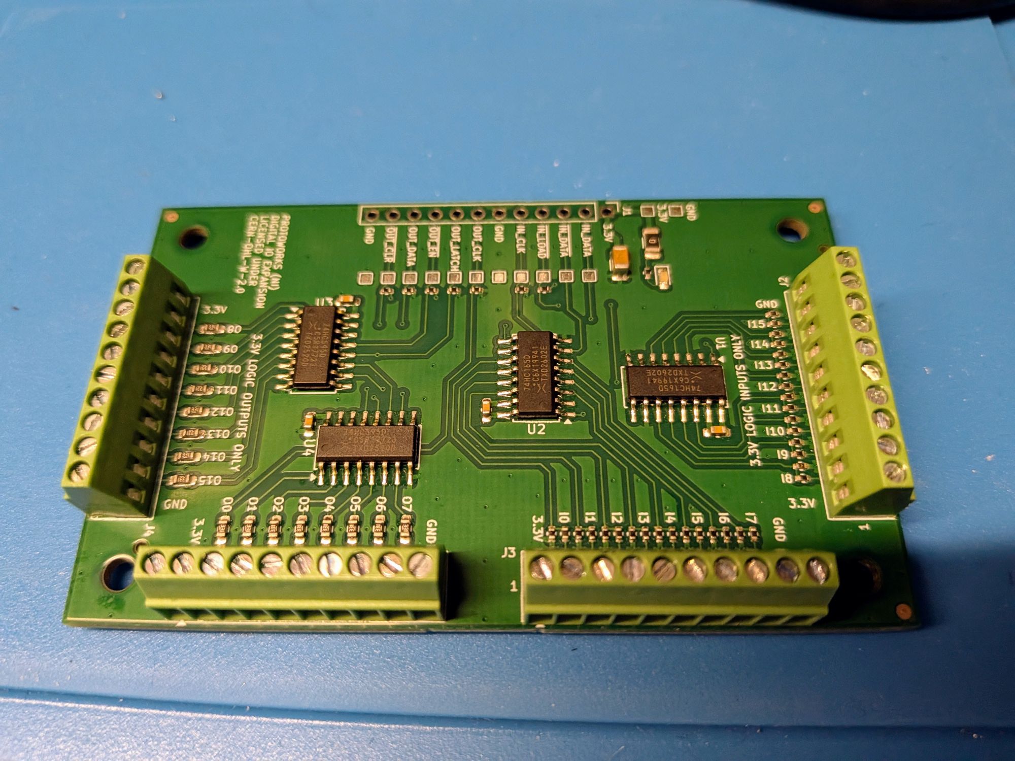
The Digital I/O Expander Board is a deterministic, shift-register-based expansion module providing 16 digital inputs and 16 digital outputs. It allows you to significantly scale the number of digital inputs and outputs available to a microcontroller using only a small, dedicated set of control lines.
Features
- 32-Channel Expansion: Adds 16 inputs and 16 outputs to your design.
- Deterministic Interface: Uses simple serial shift registers instead of bus-based GPIO expander ICs, preventing bus lockup risks and offering predictable timing.
- Robust Connections: The host microcontroller connects via a centralized 12-pin header, while all 32 external I/O channels, along with 3.3 V and GND rails, are broken out to screw terminal blocks.
Circuitry & Component Details
- Input Side: Employs 2 × 74HC165 parallel-in, serial-out shift registers.
- Output Side: Employs 2 × 74HC595 serial-in, parallel-out shift registers.
[!IMPORTANT] Rev A Silkscreen Labeling Issue: On Rev A boards, the input channel labels are reversed across each 8-input bank: * Physical input
I0is labeled asI7(and vice-versa). * Physical inputI8is labeled asI15(and vice-versa).The electrical connections are fully functional, but you must map the inputs in software or account for this reversal in your wiring. This silkscreen mapping issue has been resolved in the Rev B PCB design.
Pinout & Interface
12-Pin Control Header
| Pin | Label | Direction | Description |
|---|---|---|---|
| 1 | 3.3V | Input | Logic Supply (Typically 3.3 V) |
| 2 | INDATA | Output | Serial Data Line (74HC165) |
| 3 | /INDATA | Output | Inverted Serial Data Line (74HC165, optional spare) |
| 4 | /INLOAD | Input | Input Parallel Load line (Active Low, 74HC165) |
| 5 | INCLK | Input | Input Clock line for input shift registers (74HC165) |
| 6 | GND | Input | Logic Ground Reference |
| 7 | OUTCLK | Input | Output Clock line for output shift registers (74HC595) |
| 8 | LATCH | Input | Output Latch line to update output pins (74HC595) |
| 9 | /OUTEN | Input | Output Enable (Active Low, 74HC595) |
| 10 | OUTDATA | Input | Output Serial Data Line (74HC595) |
| 11 | /OUTCLR | Input | Master Reset / Clear (Active Low, 74HC595) |
| 12 | GND | Input | Logic Ground Reference |
Test Verification & Code
This board has been verified using a Raspberry Pi Pico 2 W running MicroPython. The following code reads the 16 inputs and mirrors their states directly onto the 16 outputs (accounting for the physical channel layout).
import machine
import time

# Initialize status LED
led = machine.Pin("LED", machine.Pin.OUT)

# Output Shift Register (74HC595) Pins
outclk = machine.Pin(1, machine.Pin.OUT)
outlatch = machine.Pin(2, machine.Pin.OUT)
_outen = machine.Pin(3, machine.Pin.OUT)
outdata = machine.Pin(4, machine.Pin.OUT)
_outclr = machine.Pin(5, machine.Pin.OUT)

# Input Shift Register (74HC165) Pins
indata = machine.Pin(6, machine.Pin.IN)
_inload = machine.Pin(8, machine.Pin.OUT)
inclk = machine.Pin(9, machine.Pin.OUT)

# Enable outputs and clear any existing register data
_outen.value(0)
_outclr.value(0)
time.sleep(0.1)
_outclr.value(1)

while True:
    led.toggle()

    # Latch the current states of physical inputs into the 74HC165 registers
    _inload.value(0)
    time.sleep(0.0001)
    _inload.value(1)

    bitstream = 0

    # Clock in the 16 bits of input data
    for i in range(16):
        readbit = indata.value()

        # Build bitstream
        if readbit:
            bitstream = bitstream | (1 << i)
        else:
            bitstream = bitstream & ~(1 << i)

        inclk.value(0)
        time.sleep(0.0001)
        inclk.value(1)

    # Latch line low to prepare for serial output transmission
    outlatch.value(0)
    outclk.value(0)
    time.sleep(0.0001)

    # Clock out the 16 bits to the 74HC595 outputs
    for i in range(16):
        outclk.value(0)
        time.sleep(0.0001)

        # Extract bit to send
        bittoset = (bitstream >> (15 - i)) & 1

        outdata.value(bittoset)
        led.value(bittoset)

        outclk.value(1)
        time.sleep(0.0001)

    # Latch the data to the physical outputs
    outlatch.value(1)